All about Silicone Controlled Rectifier SCR

SCR is the oldest & first member of the thyristor family. It is called SCR because; silicon is used for its construction and its operation as a rectifier (very low resistance in forward conduction and very high resistance in the reverse direction) and can be controlled.
It has three terminals;
1. Anode (A)
2. Cathode (K)
3. Gate (G)
The structure of SCR

The terminal connected to outer 'p' region is called Anode (A) The terminal connected to outer 'n' region is called Cathode (K)
The terminal connected to inner 'p' region is called the Gate (G) SCR is a unidirectional device. It blocks the current flow from cathode to anode.
Static V - I Characteristics of SCR.
An elementary circuit diagram for obtaining static V - 1 characteristics of SCR is shown in Fig.

The anode and cathode are connected to main source through the laod. The Gate and cathode are fed from another source 'Eg'.
The static V - I characteristics of SCR are shown below.

Va = Anode voltage
Ia = Anode current.
VBO=Forward break over Voltage.
VBR = Reverse breakdown voltage.
IG = Gate current.
IL = Latching current.
IH = Holding current.
LATCHING CURRENT (IL):
It is defined as the minimum value of anode current (1) which it must attain during turn -- on process to maintain conduction when gate signal is removed.
The gate pulse width should be chosen to ensure that the anode current rises above the latching current (IL).
HOLDING CURRENT (IH):
It is defined as the minimum value of anode current below which the SCR gets turned OFF. Latching current (IL) is more than holding current IH.
Latching current is associated with turn on process.
Holding current is associated with turn off process.
The three basic modes of operation of SCR are:
1. Forward Blocking mode.
2. Forward Conduction mode.
3. Reverse Blocking mode.
1. Forward Blocking Mode:
• When anode is at a higher potential than cathode, thyristor is said to be forward biased
It is seen from the figure that when gate circuit is open J1 J3 are forward bias but junction J2 is reverse bias.
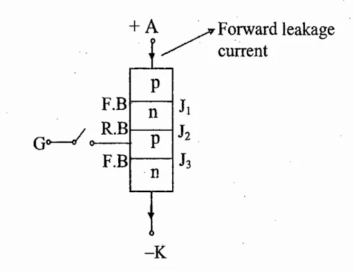
In this mode, a small current, called forward leakage current flows from anode to cathode.
OM in V-I characteristics represents the forward blocking mode of SCR.
SCR is treated as an open switch in the forward blocking mode
2. Forward Conduction Mode:
When anode to cathode forward voltage is increased with gate circuit open, reverse biased junction J2 will have an avalanche breakdown at a voltage called forward break over voltage VBO
After this breakdown, thyristor gets turned ON with point M at once shifting to N. Here NK represents the Forward conduction mode.
A thyristor can be brought from forward. blocking mode to forward conducting mode by applying,
1. A positive gate pulse between gate and cathode.
2. A forward break over voltage (Vao) across anode and cathode. Voltage drop across the SCR 'V' increases slightly with an increase in anode current. It can be seen from NK.
When cathode is made high potential with respect to anode with gate open, then the SCR is said to be reverse biased.
3. REVERSE BLOCKING MODE:

forward biased.
• A small current flows through the SCR this is called as reverse leakage current.
• This is reverse blocking mode, called the
OFF state of the SCR.
• If the reverse voltage increased, then at reverse breakdown voltage (V BR ) , an avalanche breakdown occures at J1 and J3 and the reverse current increases rapidly. (PQ)
• The SCR in the reverse blocking mode may therefore be treated as an open switch.

