Posts

Showing posts from July, 2023

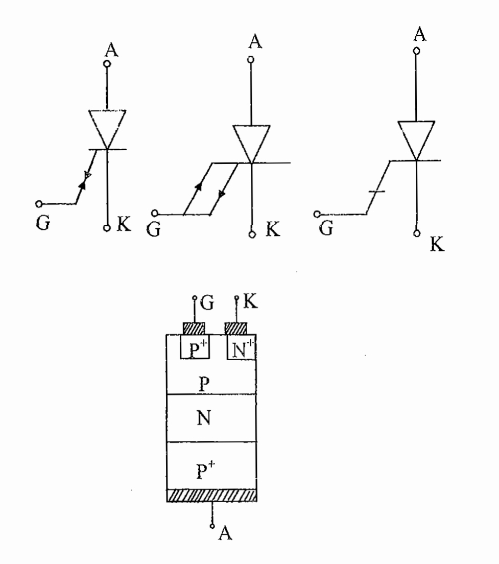
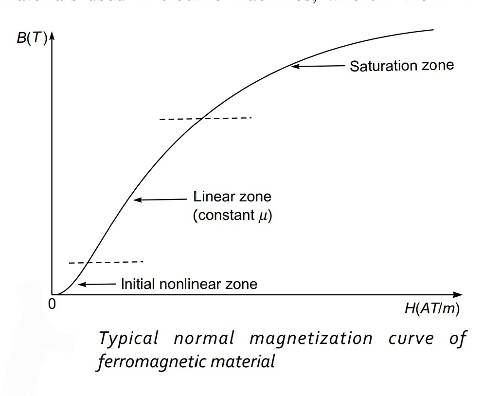
ALL ABOUT B-H RELATIONSHIP (MAGNETIZATION CHARACTERISTIC)

Image
In free space (also nonmagnetic materials), the permeability m0 is constant so that B-H relationship is linear. This, however, is not the case with ferromagnetic materials used in electric machines, wherein the B-H relationship is strictly nonlinear in two respects— saturation and hysteresis. Hysteresis non-linearity is the double valued B-H relationship exhibited in cyclic variation of H (i.e. exciting current). This nonlinearity is usually ignored in magnetic circuit calculations and is important only when current wave shape and power loss are to be accounted for. This is discussed in Sections 2.3 and 2.6. A typical normal B-H relationship (magnetization characteristic) for ferromagnetic materials is shown It has an initial nonlinear zone, a middle almost linear zone and a final saturation zone in which B progressively increases less rapidly with H compared to the linear zone. In the deep saturation zone, the material behaves like free space. Due to considerati...

MAGNETIC CIRCUIT AND INDUCTION

Image
1. Magnetic Circuit Calculations: Normally magnetic circuit calculations involve two types of problems. In the first type of problem it is required to determine the excitation (mmf ) needed to establish a desired flux or flux density at a given point in a magnetic circuit. This is the normal case in designing electromechanical devices and is a straight forward problem. In the second category, the flux (or flux density) is unknown and is required to be determined for a given geometry of the magnetic circuit and specified mmf. This kind of problem arises in magnetic amplifiers wherein this resultant flux is required to be determined owing to the given excitation on one or more control windings. A little thought will reveal that there is no direct analytical solution to this problem because of the non-linear B-H characteristic of the magnetic material. Graphical/numerical techniques have to be used in obtaining the solution of this problem. 2. Leakage Flux: In all practica...

GTO (GATE TURN OFF THYRISTOR)

Image
A GTO is a more versatile power semiconductor device. It is like a conventional thyristor but with added features in it. A GTO can be easily turned off by a negative gate pulse of appropriate amplitude. Thus a GTO is a device that can be turned on by a positive gate current and turned off by a negative gate current at its gate cathode terminals. Self- turn off capability of GTO makes it the most suitable device for inverter and chopper applications. The four layers of GTO have different doping levels indicate by P+nP+n+ Transistor Q1 is P+ NP+ type and Q2 is NP+ N+. Emitter of Q1 as anode and Emitter of Q2 as cathode. Turns on process: A GTO is turned on by applying a positive gate current Ig in the direction shown. Current gains a1 and a2 begins to rise and when a1 + a2 = 1 saturation level is reached and GTO is turned ON. Turn off process: For initiating the turn off process, Q2 must be brought out of saturation. The gate current ig1 is given in opposite side....

PROTECTION OF SCR

Image
di/dt Protection: When a thyristor is forward biased and is turned ON by a gate pulse, conduction of anode current begins. If the rate of rise of anode current (di/dt) is very fast compared with the spreading velocity of charges a local hot spots will be formed. This localised heating may destroy the thyristor. Therefore, the di/dt rate of rise of anode current at the time of turn on must be kept below the specified limiting value by using a small inductor, called di/dt inductor, in series with the anode circuit. dv/dt Protection: If the rate of rise of applied voltage across thyristor is high, the device may get turned on. Such phenomena of turning on a thyristor, called dv dt turn on must be avoided as it leads to false operation. False turn on of an SCR by large- dv dt even with out application of gate signal can be prevented by using a Snubber circuit in parallel with the device.

SWITCHING CHARACTERISTICS OF SCR

Image
SWITCHING CHARACTERISTICS DURING TURN-ON: SCR Turn on time is defined as the time during which SCR changes from forward blocking mode to final on-state. Total turn on time can be divided into three Total turn on intervals; (i) Delay time (td). (ii) Rise time (tr) (iii)Spread time (tp) Turn on time = ta + tr + tp Delay time (td): The delay time (td) is the time between the instant at which gate current reaches 0.9 Ig to the instant at which anode current reaches 0.1 Ia. Here Ig and Ia are respectively the final values of gate and anode currents. (or) The delay time (td) may also be defined as the time during which anode voltage falls from Va to 0.9 Va where Va= initial value of anode voltage. (or) The time during which anode current rises from forward leakage current to 0.1 Ia where la final = value of anode current. Rise time (tr): The time taken by the anode current to rise from 0.1 la to 0.9 Ia. (or) The rise time is also defined as the time required for the forward block...

All about Silicone Controlled Rectifier SCR

Image
SCR is the oldest & first member of the thyristor family. It is called SCR because; silicon is used for its construction and its operation as a rectifier (very low resistance in forward conduction and very high resistance in the reverse direction) and can be controlled. It has three terminals; 1. Anode (A) 2. Cathode (K) 3. Gate (G) The structure of SCR The terminal connected to outer 'p' region is called Anode (A) The terminal connected to outer 'n' region is called Cathode (K) The terminal connected to inner 'p' region is called the Gate (G) SCR is a unidirectional device. It blocks the current flow from cathode to anode. Static V - I Characteristics of SCR. An elementary circuit diagram for obtaining static V - 1 characteristics of SCR is shown in Fig. The anode and cathode are connected to main source through the laod. The Gate and cathode are fed from another source 'Eg'. The static V - I characteristics of SC...

All about Thyristor

Image
The name 'thyristor' is derived by a Combination of the capital letters from THYRatron and transISTOR. International Electrotechnical Commission (IEC) in 1963 decided the definition of Thyristor as under: (i) It constitutes three or more pn junctions. (ii) It has two stable states, an ON - State and an OFF State and can change its state from one to another. Thyristor is a four layer, three - junction, p - n - p- n semiconductor switching device.